For my Electronics class, I took on a project of designing a buck converter, utilizing a 555 timer as the PWM signal. The expectation was that the output of the buck converter would be adjustable through the use of a variable potentiometer, in which the maximum output voltage would occur when the potentiometer is in its most resistive state and the minimum output voltage would occur in its least resistive state. The circuit that I designed utilizes a NE555 timer, a 100kOhm potentiometer, two 1kOhm resistors, a 1MOhm resistor, a 10kOhm resistor, two 1N4148 diodes, a 100pF capacitor (ceramic), two 10μF capacitors (one ceramic, one electrolytic), a 470μH inductor, a 1N5819 schotty diode, and a 9.1V zener diode.
Theory:
555 Timer:
To begin with understanding how this circuit works, it will be helpful first to establish how a 555 timer works, specifically when it is in astable operation. The core of how a 555 timer works is through capacitor charging and discharging relationships and comparators. Taking a look at the picture below depicting the internal components of how a 555 timer operates, we can see what causes a 555 timer to operate in its astable mode (Figure 1):
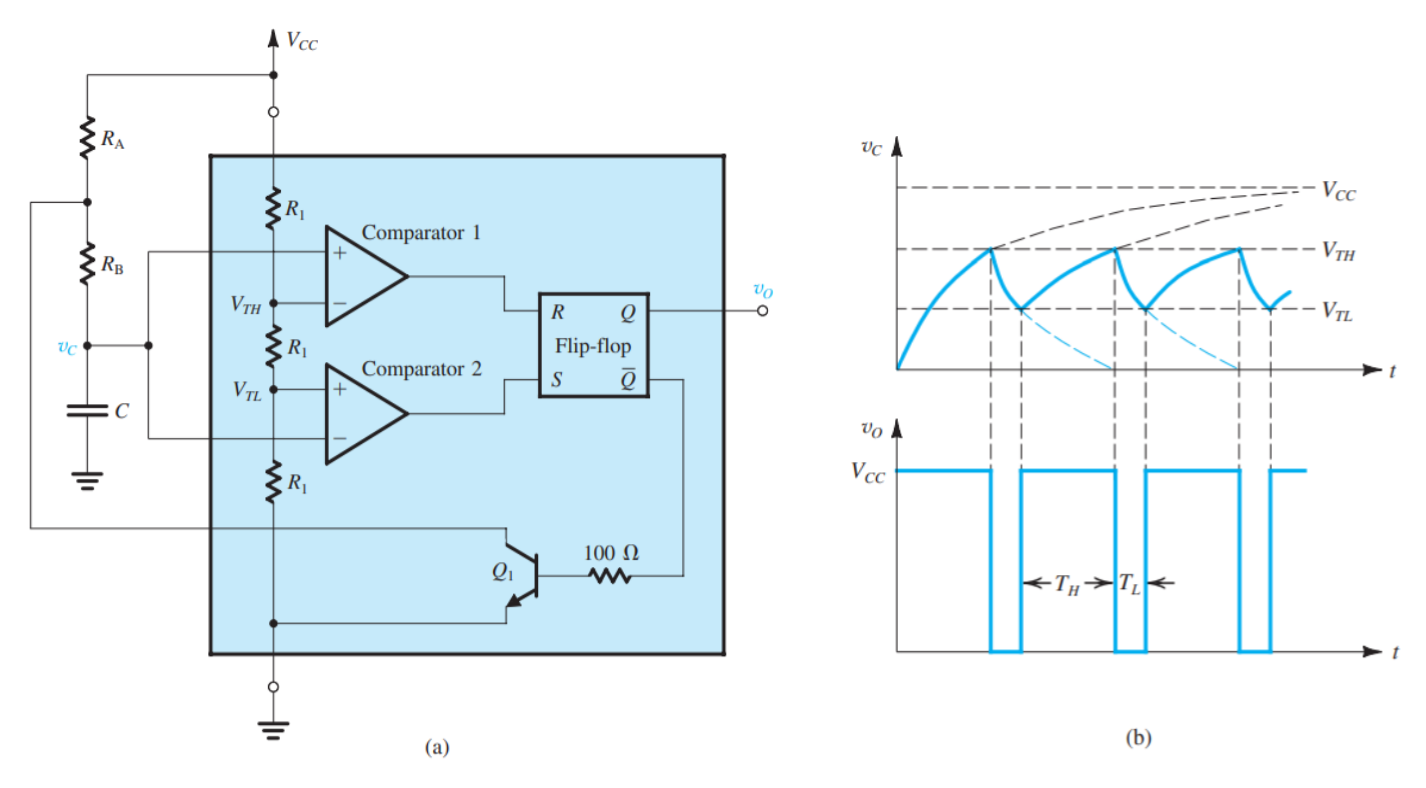
Figure 1: Internal component behavior of 555 timer, sourced from Microelectronic Circuits (Sedra and Smith) [1].
The output behavior (Vo) of a 555 timer can be expressed through the following four parameters: Frequency (f), which represents the number of times per second the waveform completes a period, Duty Cycle (D), which represents the ratio of the amount of time the output is high divided by one period of the waveform, Time High (TH), which represents the amount of time that the waveform is high over a period, and Time Low (TL), which represents the amount of time that the waveform is low over a period. An example of the analysis used to determine the resistors (RA & RB) needed for a 555 timer operating in astable mode, changing at a frequency of 20kHz, a duty cycle of 80%, utilizing a 680pF capacitor is shown below (Figure 2):
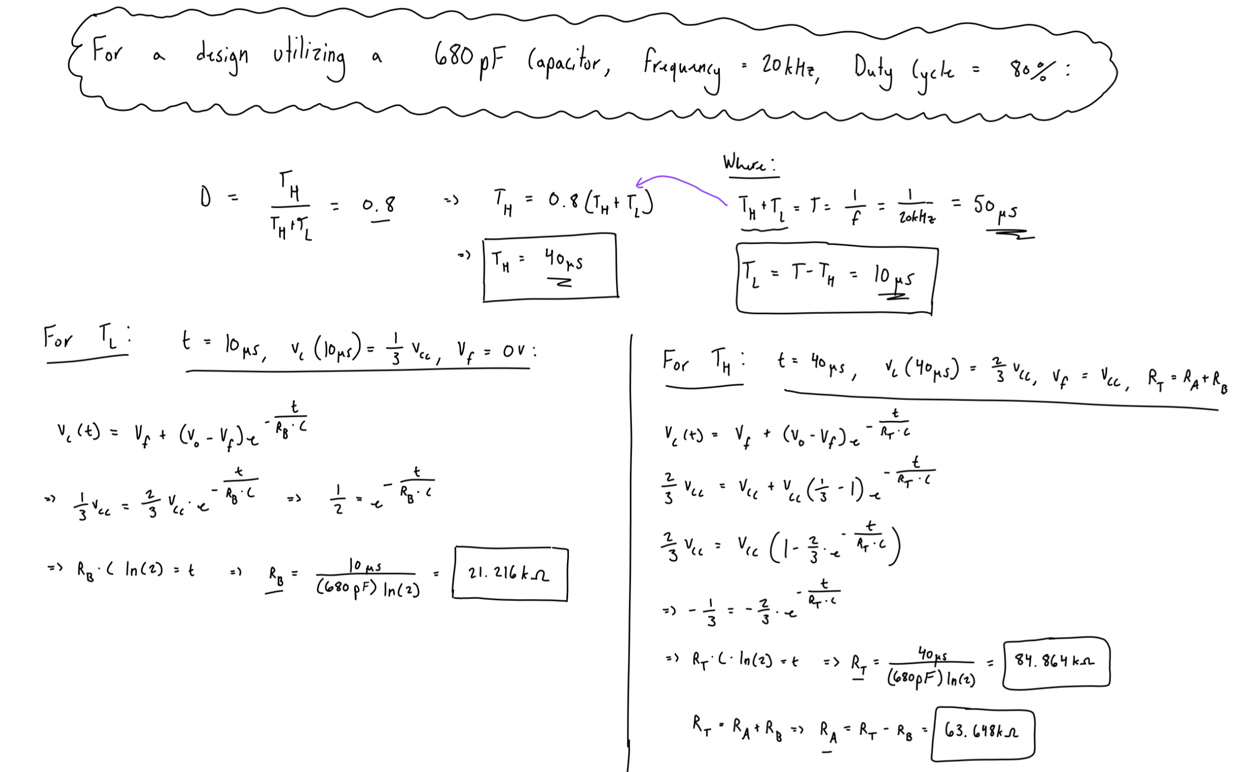
Figure 2: Design example of 555 timer with D = 0.8, f = 20kHz, and C = 680pF.
This analysis utilizes the equation of natural charging and decaying of a capacitor’s voltage to determine the desired characteristics of our 555 timer circuit. This analysis isn’t needed for every design iteration of a 555 timer PWM generator, as we can instead use some helpful almost shortcut equations for the desired parameters, shown in the below figure (Figure 3):
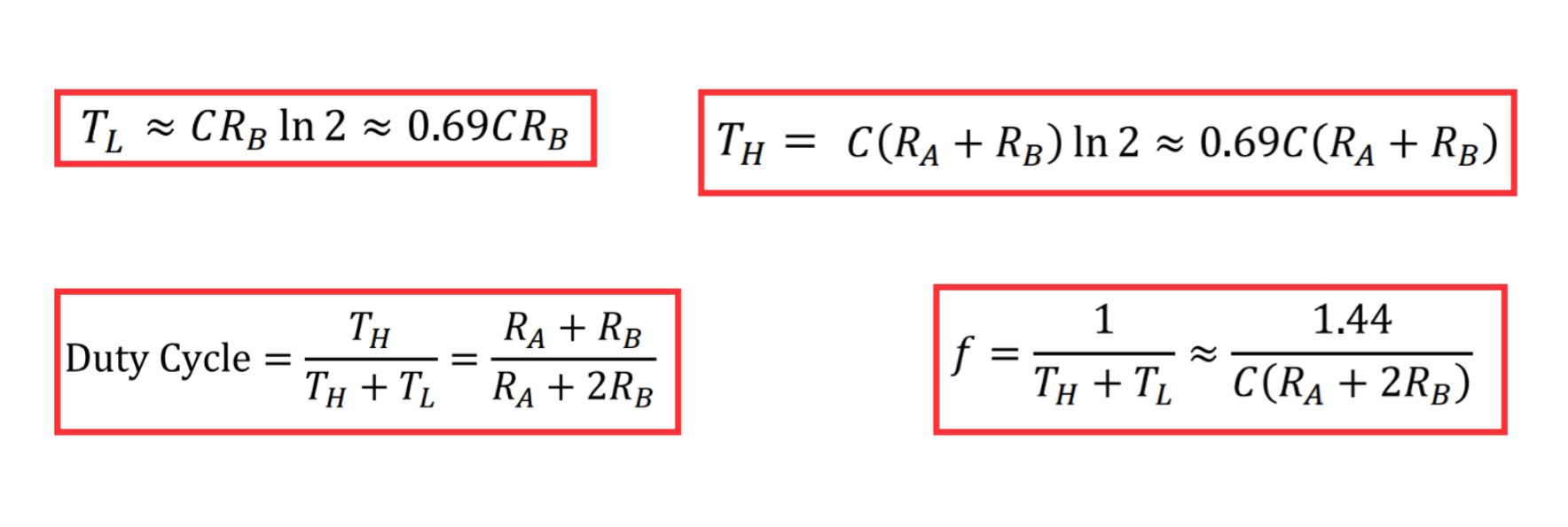
Figure 3: Equations describing parameters of 555 timer based on components, sourced from Microelectronic Circuits (Sedra and Smith) [1].
There is however a catch to using this circuit configuration for an astable mode 555 timer. The duty cycle for this setup can never be below 50%, as if we take RA = 0Ohm, duty cycle = 0.5, if RA = ꝏ, duty cycle ≈ 1, if RB = 0, duty cycle = 1, and if RB = ꝏ, duty cycle ≈ 0.5. To achieve a duty cycle lower than 50%, another circuit configuration has to be used to achieve this behavior. The circuit layout is shown in the below figure (Figure 4):
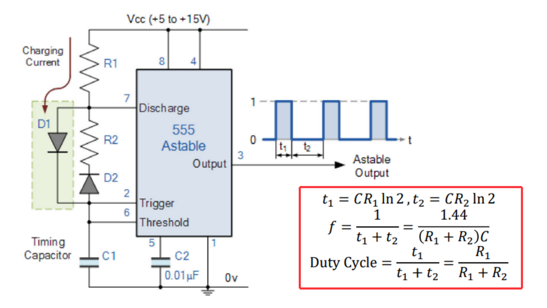
Figure 4: 555 timer circuit that allows for duty cycles less than 0.5, sourced from lecture [2].
Buck Converter:
A buck converter is a DC-DC voltage converter that takes a higher input voltage and steps it down to a lower output voltage. The purpose behind this being that the lower output voltage allows for a higher output current due to the law of conservation of power (Pin = Pout, thus Vin*Iin = Vout*Iout). Due to buck converters mainly being comprised of inductive/capacitive components, buck converters are typically very efficient, so the assumption that Pin = Pout is typically a good assumption. Thus, we can say that the current output of the buck converter is directly equal to Pin / Vout. The general circuit for a buck converter is shown in the figure below (Figure 5):
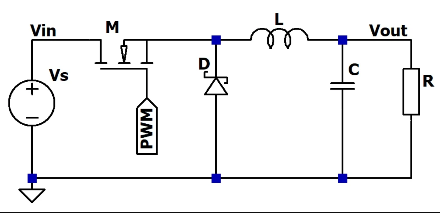
Figure 5: General circuit schematic for a buck converter, sourced from [3].
Equations and more information about the operation and behavior of a standard buck converter can be seen in the below figures (Figures 6 & 7):
-
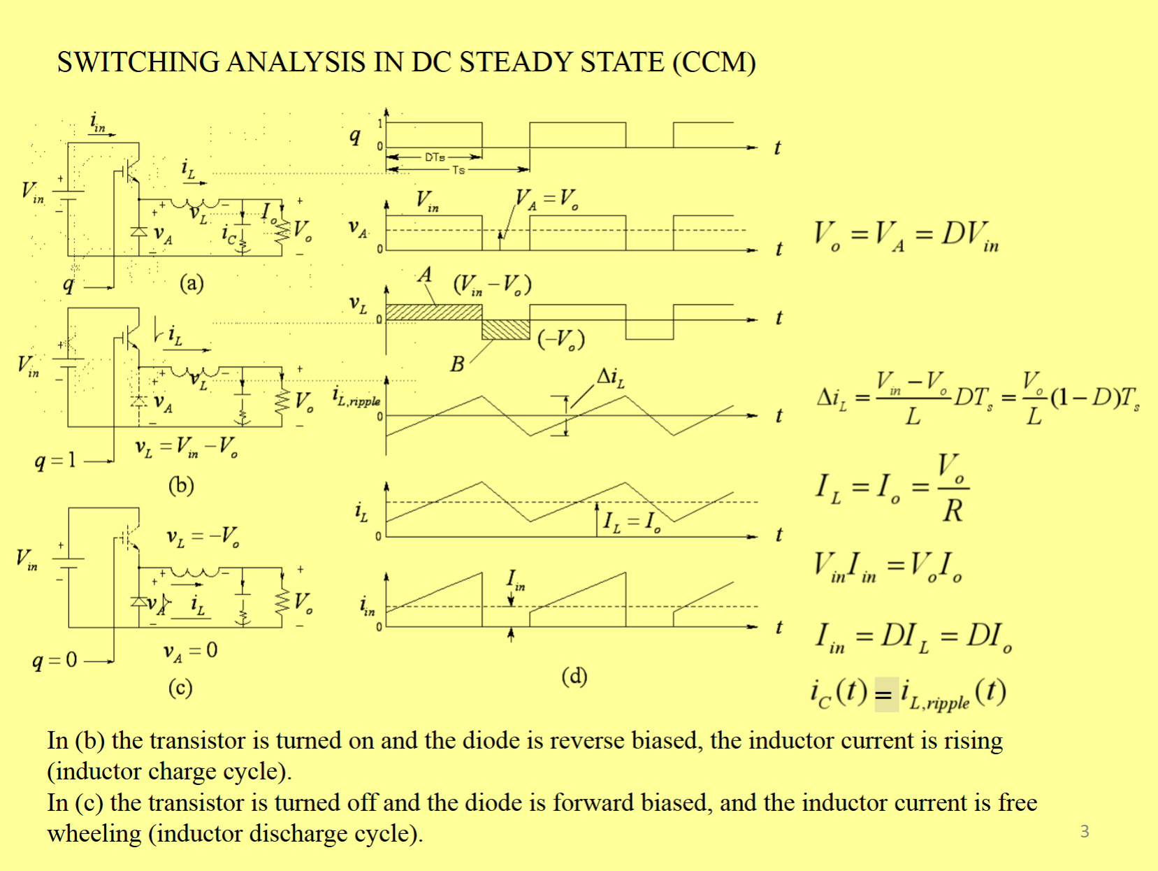
- Figure 6: Theoretical waveform behavior of a general buck converter, sourced from [4].
-
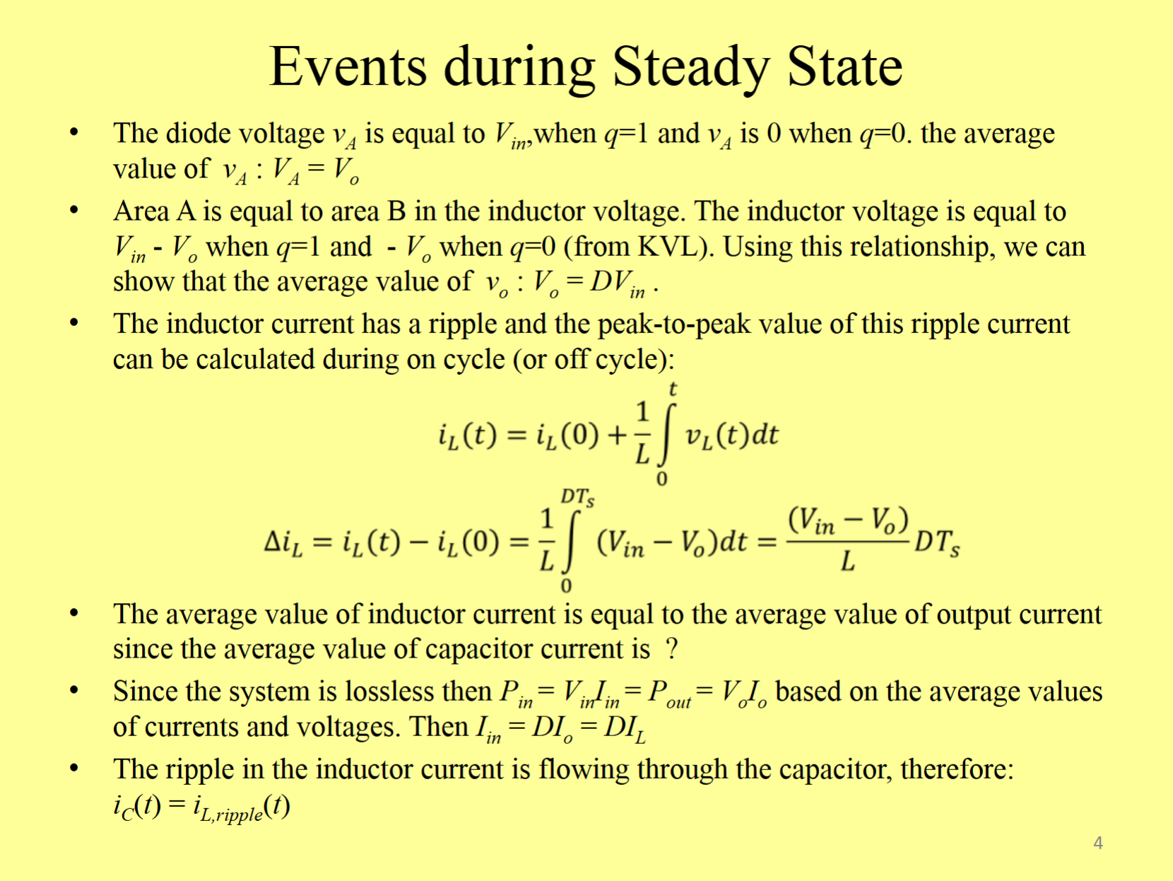
- Figure 7: Equations and information describing general buck converter behavior, sourced from [4].
From the above listed equations, we can see that current ripple is directly proportional to duty cycle, so in order to vary the output current (and therefore output voltage), duty cycle must be changed.
Design:
In order to meet the desired specifications for this design project, I knew that I would need to use a 555 timer configuration that would allow for a duty cycle less than 0.5, as supplying a very small duty cycle to a buck converter results in close to zero volt output. I knew I also needed to be able to adjust something with the circuit so that the PWM signal provided a very high duty cycle, preferably around 0.99. To accomplish this, I used a variable potentiometer that would adjust the RA and RB values such that when fully rotated clockwise, RA would be a magnitude of ~101 times smaller than the value of RB and when rotated fully counterclockwise, RB would be a magnitude of ~101 times smaller than RA. What this means is that when RA is in its least resistive state, the duty cycle of the 555 timer is essentially zero and when its in its most resistive state, the duty cycle of the 555 timer is essentially one. This gives a nice linear range of the output voltage of the buck converter from 0V to (theoretically) Vcc.
The circuit that I created for the PWM signal generation side for the buck converter utilized a 100kOhm potentiometer, two 1kOhm resistors, a 100pF capacitor (smallest I had access to), and two 1N4138 diodes. This circuit theoretically yields a frequency value of 141kHz, a duty cycle of 0.0098 for a P_RA (potentiometer RA variable) value of 0Ohm and a duty cycle of 0.9902 for a P_RB (potentiometer RB variable) value of 0Ohm. The full circuit schematic of the 555 timer portion of this DC-DC converter can be seen in the figure below (Figure 8):
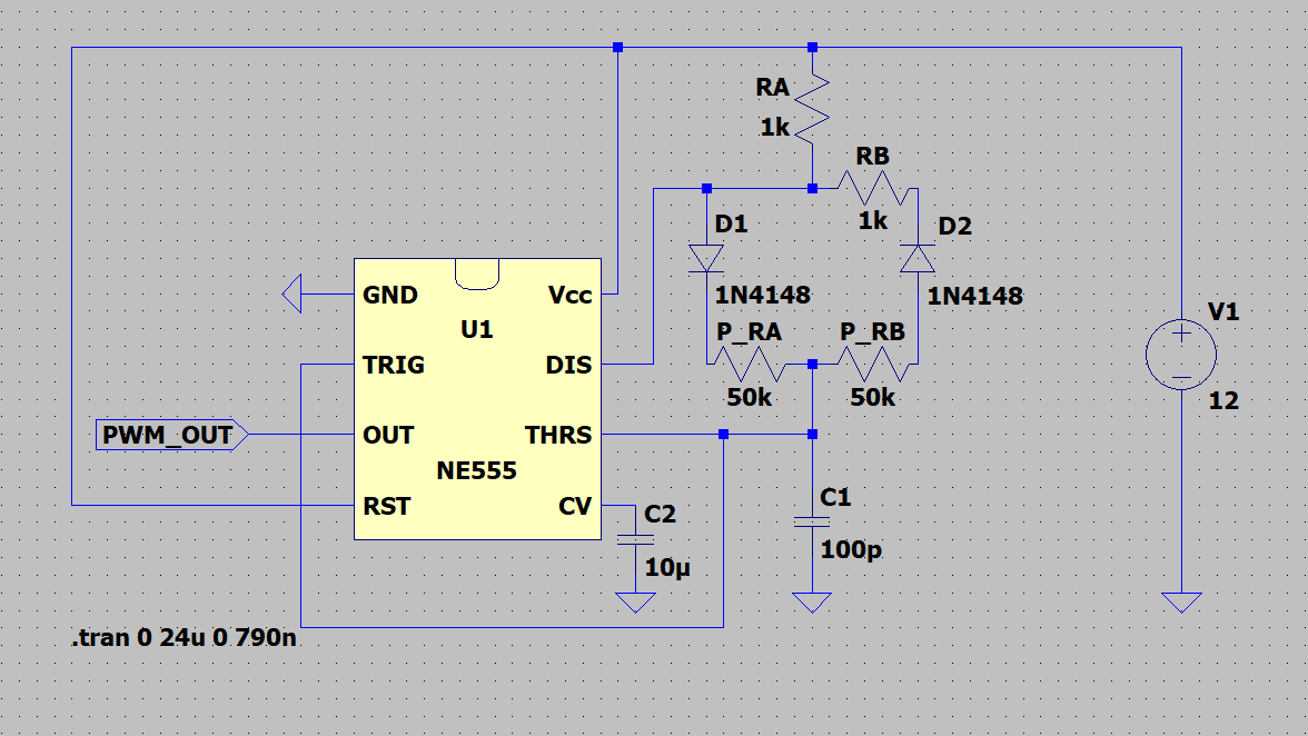
Figure 8: Circuit schematic for the 555 timer PWM generator portion of this buck converter.
For the DC stepping down portion of the circuit, I utilized a 1Mohm resistor, a 1N5819 diode, a 470uH inductor, a 10uF capacitor (polarized), a 10kOhm resistor, a 9.1V zener diode, and an FQP30N06L MOSFET. I used the largest inductor that I had access to to try and minimize output current ripple. The stepping down portion of the circuit can be seen in the figure below (Figure 9):
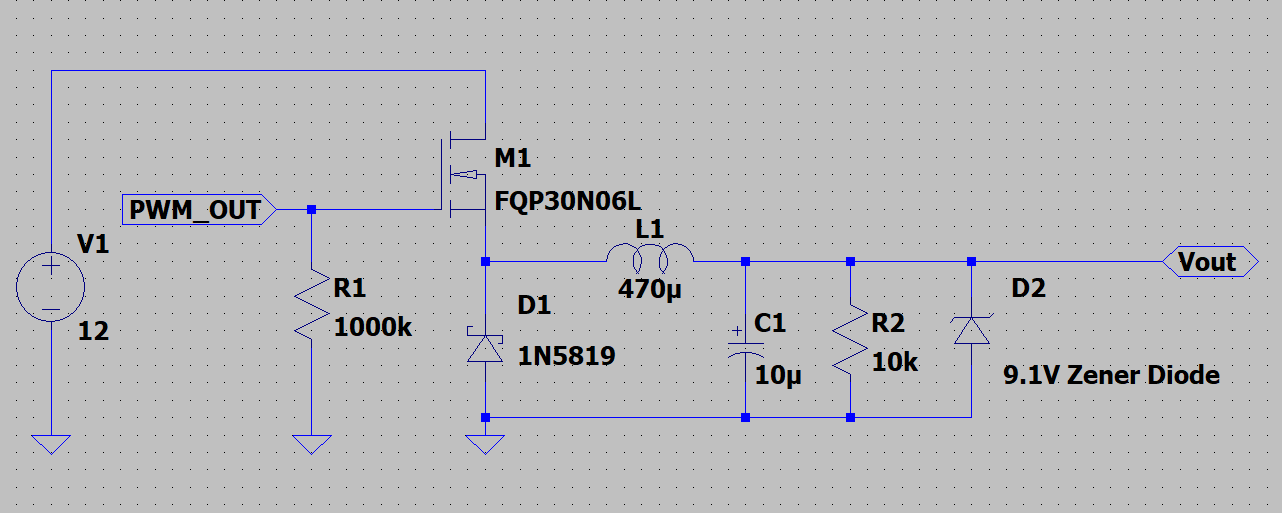
Figure 9: Circuit schematic for the “buck” portion of this buck converter.
Results:
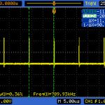
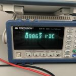
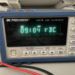
To verify the functionality of the buck converter, I captured the DMM output voltage values corresponding to the minimum and maximum duty cycles of the 555 timer. The input voltage for the circuit was 12V and at a duty cycle of approximately 0.36%, the measured output voltage was around 0.98V. This measured output voltage roughly lines up with the expected behavior of the buck converter, as the output voltage should effectively go to 0V when the PWM signal has a low duty cycle. At a duty cycle of approximately 96% (without the zener diode), the measured output voltage was around 9.5V. This output voltage differs quite a bit from the expected output voltage of ≈ 11.5V, which is likely due to non-idealities in the circuit. Some of these could include: losses in voltage due to resistance of the MOSFET, losses in the inductor/capacitor, and losses due to parasitic resistances from the breadboard. The following figures show the observed waveforms and measured DMM values for the physical circuit (Figures 10-15):
-
- Figure 10: Output waveform of converter at a duty cycle of 0.36%.
-
- Figure 11: Measured output voltage using a DMM with converter duty cycle = 0.36%.
-
- Figure 12: Output waveform of converter at a duty cycle of 96%.
-
- Figure 13: Measured output voltage using a DMM with converter duty cycle = 96%.
-
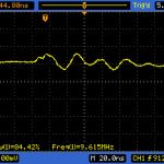
- Figure 14: Ripple behavior of the output voltage.
-
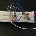
- Figure 15: Picture of the actual circuit hooked up together on a breadboard.
Overall, the results demonstrated that the buck converter that I designed successfully stepped down a 12V input to a controllable output voltage of ≈ 1-9V, controlled entirely by a 555 timer PWM circuit.
References:
[1] A.S. Sedra and K. C. Smith, Microelectronic Circuits, 7th ed. New York, NY, USA: Oxford University Press, 2015.
[2] B. Yang, “Multivibrators” EE 331: Fundamentals of Electronics and Semiconductors. Western Carolina University, Fall 2024. (Lecture Notes)
[3] TAVO Tech, “How a Buck Converter Works,” TAVO Tech. [Online]. Available: https://tavotech.com/how-a-buck-converter-works/.
[4] H. Karayaka, “MOSFET Buck Converter”, EE 312: Systems and Electronics Lab. Western Carolina University, Spring 2025. (Lab Session).
Recent Comments