For my Power Electronics class, I took on the project of designing a boost converter circuit. The specifications of the project were that the converter was to have an adjustable output voltage dependent on the state of a variable potentiometer. The maximum output voltage was to occur when the potentiometer is in its most resistive state and the minimum output voltage was to occur in its least resistive state. The circuit that I designed uses a similar signal triggering mechanism to that of my previous buck converter project, in which a 555 timer is utilized as the switching signal. Since my last post, my LTspice skills have significantly improved, and I have learned how to import certain spice models to get the correct behavior out of the circuits that I use. In this new project, I’ve imported the FQP30N06 spice model from https://www.onsemi.com/download/models/lib/fqp30n06.lib. This spice model allows for the proper modeling of the FQP30N06 Mosfet, with all of its characteristics built in. This model is extremely close to the real-world model that is observed.
Theory:
555 Timer:
To begin with understanding how this circuit works, it will be helpful first to establish how a 555 timer works, specifically when it is in astable operation. The core of how a 555 timer works is through capacitor charging and discharging relationships and comparators. Taking a look at the picture below depicting the internal components of how a 555 timer operates, we can see what causes a 555 timer to operate in its astable mode (Figure 1):
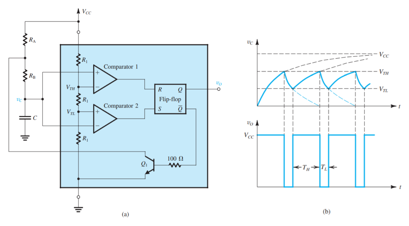
Figure 1: Internal component behavior of 555 timer, sourced from [1].
The output behavior (Vo) of a 555 timer can be expressed through the following four parameters: Frequency (f), which represents the number of times per second the waveform completes a period, Duty Cycle (D), which represents the ratio of the amount of time the output is high divided by one period of the waveform, Time High (TH), which represents the amount of time that the waveform is high over a period, and Time Low (TL), which represents the amount of time that the waveform is low over a period. An example of the analysis used to determine the resistors (RA & RB) needed for a 555 timer operating in astable mode, changing at a frequency of 45kHz, a duty cycle of 50%, utilizing a 100pF capacitor is shown below (Figure 2):
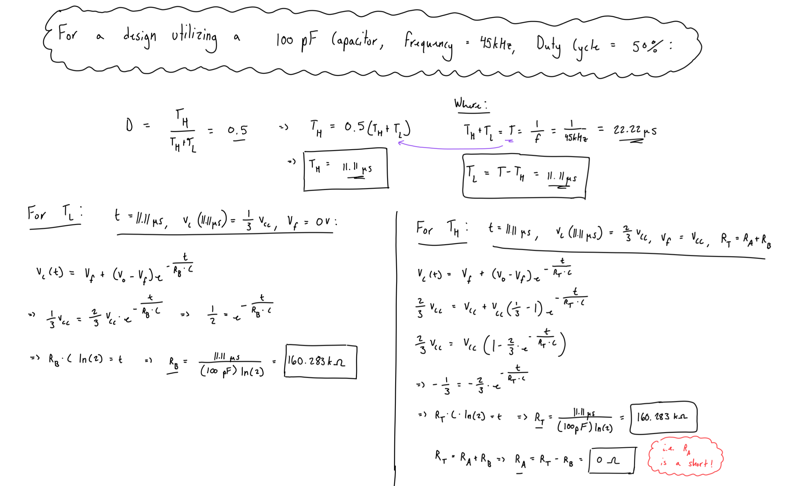
Figure 2: Design example of 555 timer with D = 0.5, f = 45kHz, and C = 100pF.
This analysis utilizes the equation of natural charging and decaying of a capacitor’s voltage to determine the desired characteristics of our 555 timer circuit. This analysis isn’t needed for every design iteration of a 555 timer PWM generator, as we can instead use some helpful shortcut equations for the desired parameters, shown in the below figure (Figure 3):
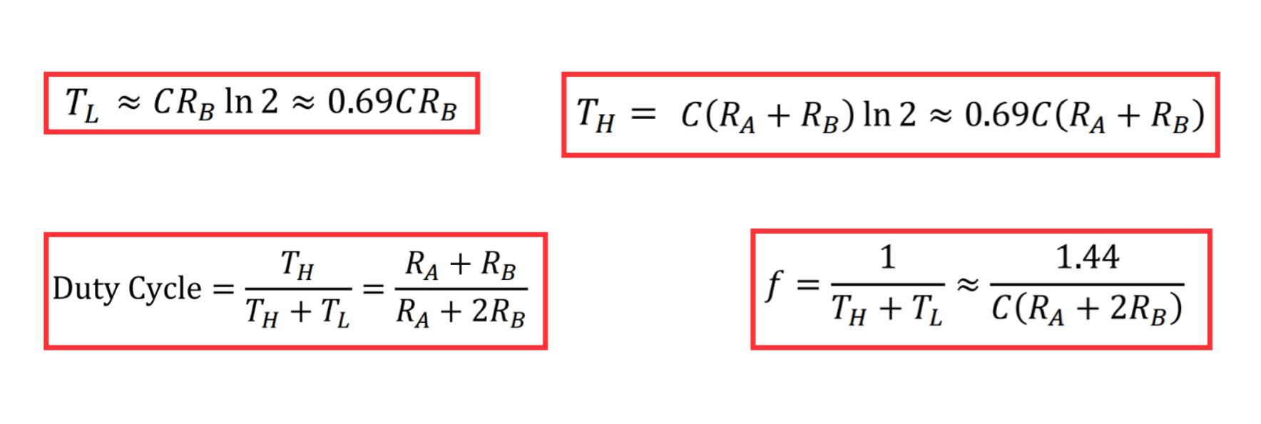
Figure 3: Equations describing parameters of 555 timer based on components, sourced from [1].
There is however a catch to using this circuit configuration for an astable mode 555 timer. The duty cycle for this setup can never be below 50%, as if we take RA = 0Ohm, duty cycle = 0.5, if RA = ꝏ, duty cycle ≈ 1, if RB = 0, duty cycle = 1, and if RB = ꝏ, duty cycle ≈ 0.5. To achieve a duty cycle lower than 50%, another circuit configuration has to be used to achieve this behavior. The circuit layout is shown in the below figure (Figure 4):
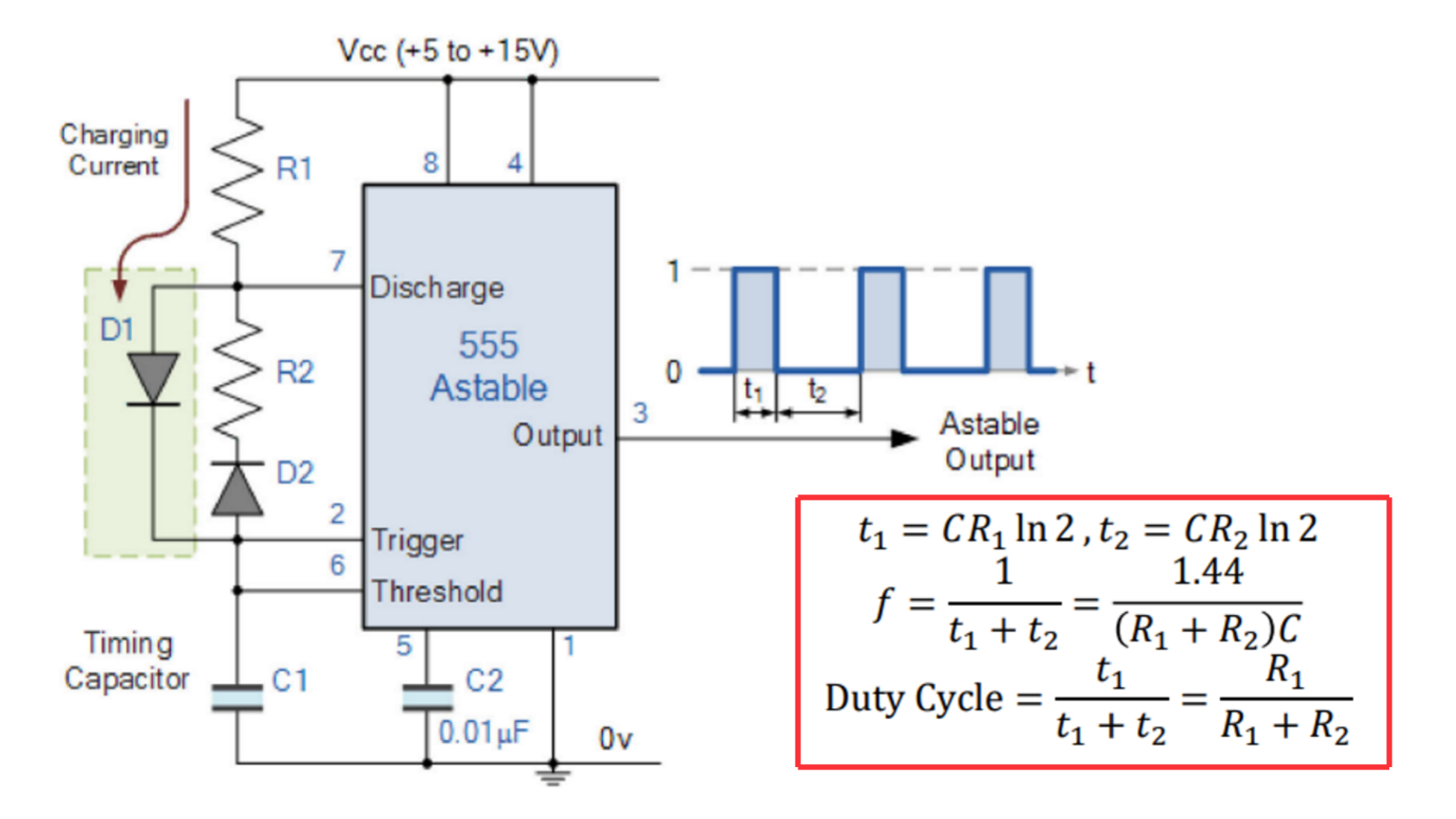
Figure 4: 555 timer circuit that allows for duty cycles less than 0.5, sourced from [2].
Boost Converter:
A boost converter is a DC-DC voltage converter that takes a lower input voltage and “boosts” it up to a higher output voltage. The need for a boost converter is facilitated in power electronics as it is an efficient and simple method to create a higher output voltage from a lower input voltage. Due to their component composition and switching behavior, boost converters are extremely efficient, so it is typically assumed that Pin ≈ Pin, thus giving an approximate output current as being equal to Pin / Vout. The general circuit for a boost converter is shown in the figure below (Figure 5):
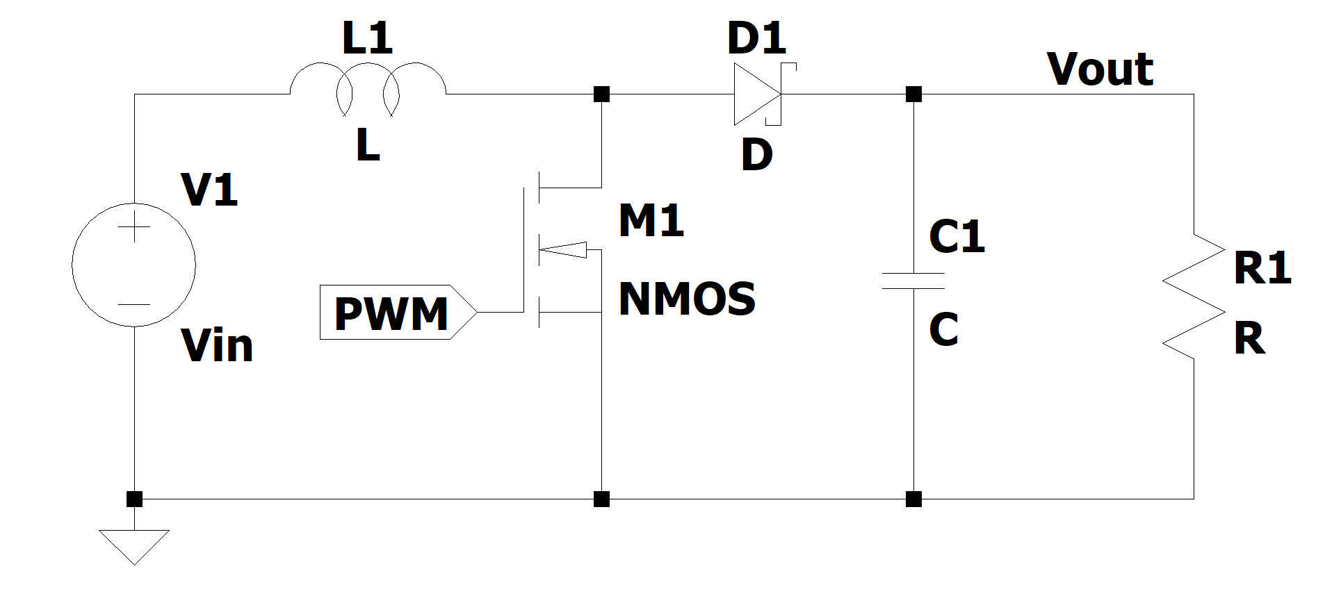
Figure 5: General circuit schematic for a boost converter.
The operating behavior of a boost converter is through switching action, an inductor, and a filtering capacitor. To achieve this switching action, the circuit takes advantage of the cutoff and saturation region of a transistor (N-type MOSFET typically). When a large enough positive voltage is applied to the input pin on the transistor, current begins to flow through the inductor, storing energy in its magnetic field. During this charging phase, the inductor opposes the sudden change in current, allowing it to ramp up gradually. In the absence of an input voltage (0V) on the input pin of the transistor, the transistor turns off and in turn causes the inductor’s stored magnetic field to begin to collapse. In this state, the inductor acts as source of current for the output load, with a filtering capacitor placed in parallel to filter the DC component of the switching action. This process repeats for every period of the PWM signal.
Equations and output waveforms of a boost converter’s behavior can be seen in the figure below (Figure 6):
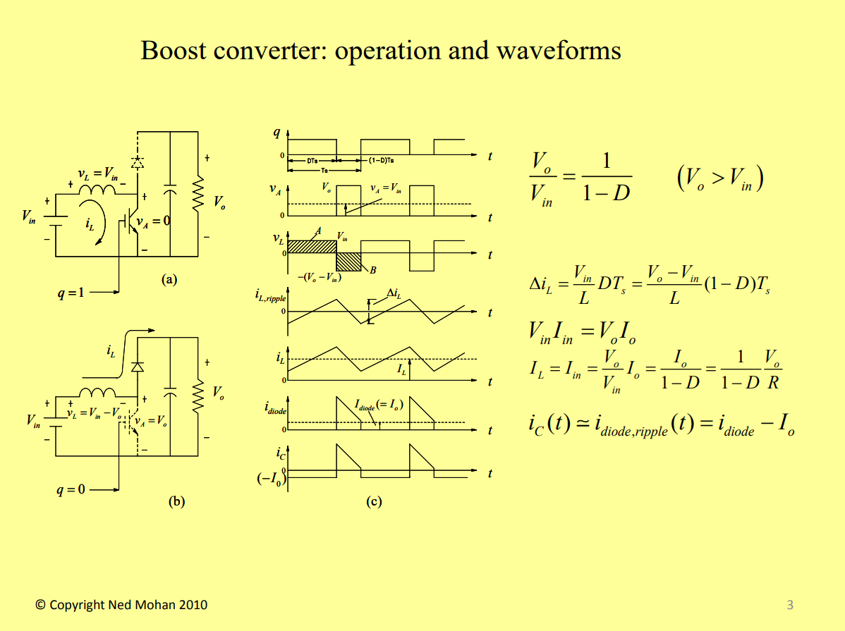
Figure 6: Theoretical waveform behavior of a general boost converter, sourced from [5].
Design:
For this project, I wanted to design a buck converter that could supply a 200Ω load at a maximum output voltage of 12V with a ripple voltage < 1.7% (20mV), given an input voltage of 5V and a switching frequency of 60kHz. The input and output parameters for this were chosen arbitrarily, but these values are typical for a power boost converter. To achieve the design for this, design calculations had to be performed to determine the proper inductor, capacitor, and ripple values. To achieve an output voltage of 12V, an equation relating output voltage to input voltage and duty cycle was used. For an input voltage of 5V and an output of 12V, it was determined that a duty of 0.583 would achieve this voltage output. At an output voltage of 12V and a load of 200Ω, the average output current would be 60mA, and via the previously found duty cycle and a formula relating output current to input current and duty cycle, it was found that at an output of 12V, the input current would be 144mA. To deal with some of the nasty effects that can come with a small inductor ripple current while also keeping a good compromise on inductor sizing, the decision was made to design for a ripple current of 30% of the average input current (read more on that here: https://www.analog.com/en/resources/technical-articles/selecting-the-right-inductor-current-ripple.html). This yielded a ripple current of ~43mA. Based on the ripple current, input voltage, duty cycle, and switching frequency, the inductance needed to have these values was an inductor of 1.125mH. To achieve a ripple voltage of 20 mV, a calculation was performed using a formula that relates the required capacitance to the specified output current, duty cycle, frequency, and ripple voltage. This yielded a capacitor value of 29.15μF. The calculations and formulas used in these calculations can be seen below (Figure 7):
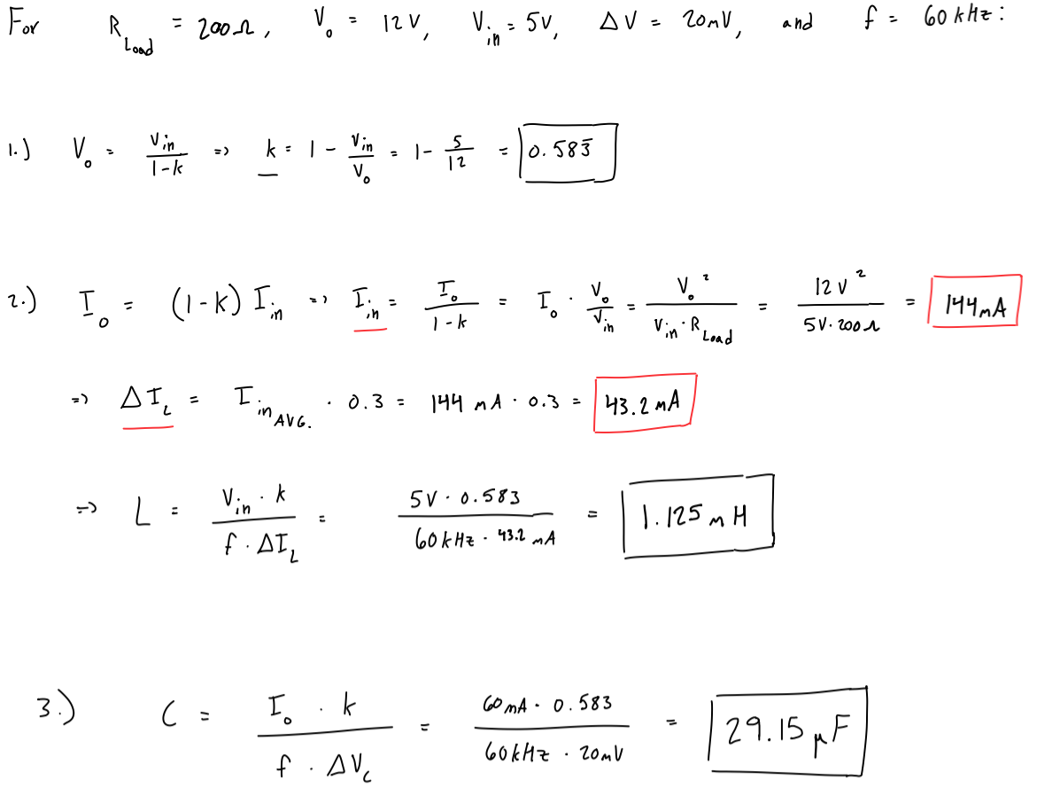
Figure 7: Design calculations to determine proper inductor and capacitor values for specified load, output voltage, ripple, and switching frequency.
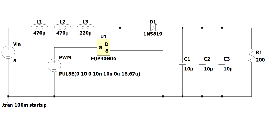
Using the above design calculations as a guideline, I constructed a circuit schematic for the boost portion of the boost converter, utilizing circuit components that I had readily available to me. The components that I comprised the circuit from consisted of a FQP30N06L (N-type MOSFET) for the transistor, two 470μH inductors, one 220μH inductor, one 1N5819 schottky diode, three 10μF ceramic capacitors, and a 200Ω load resistor. The schematic for the overall boost circuit and its resultant output waveforms for theoretical duty cycle of 0.583 and 0 are shown in the figures below (Figures 8-11):
-
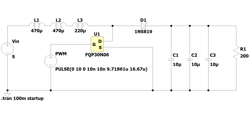
- Figure 8: Schematic for Boost Converter with D = 0.583.
-
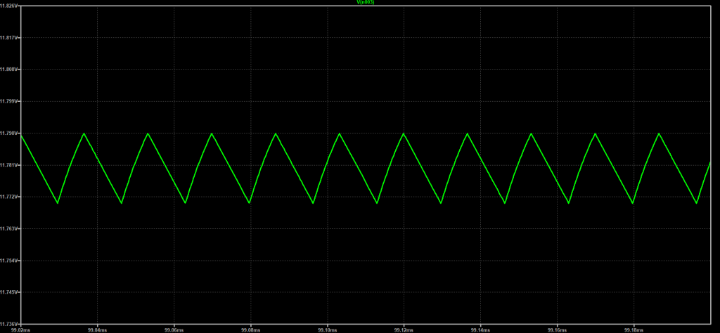
- Figure 9: Output waveform for Boost Converter circuit with D = 0.583.
-
- Figure 10: Schematic for Boost Converter with D = 0.
-
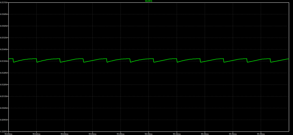
- Figure 11: Output waveform for Boost Converter circuit with D = 0.
To achieve the maximum switching speed and duty cycle found above, I knew that the 555 timer configuration would have to yield a duty cycle ranging from ~0 to 0.583 at a frequency of 60kHz. To accomplish the variability of duty cycle, a potentiometer was used to adjust the RA and RB values such that when fully rotated clockwise, the maximum duty cycle of ~0.583 is achieved and when fully rotated counterclockwise, the minimum duty cycle of ~0 would be achieved. To determine the corresponding values needed to get this duty cycle range and frequency, the equations from Figure 4 were used to calculate appropriate resistor and capacitor values. The calculations for this are shown in the figure below (Figure 12):
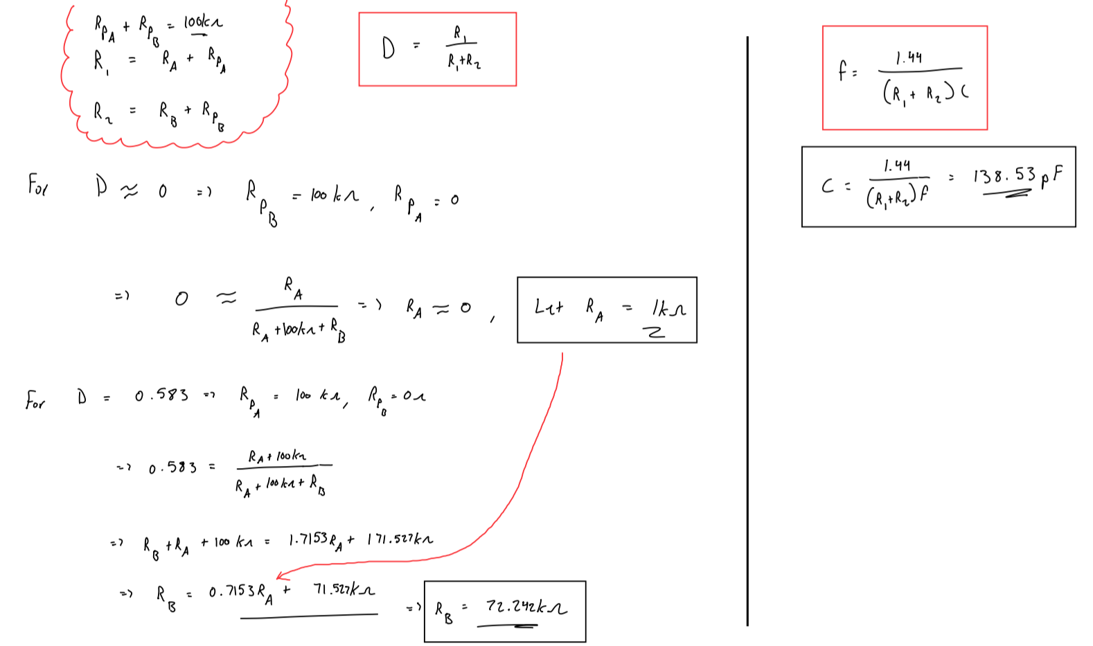
Figure 12: Design calculations to determine proper capacitor and resistor values for specified duty cycle and frequency of 555 timer.
Given these calculations, I created a circuit for the PWM signal generation side of the buck converter utilizing a NE555 timer IC, one 100kΩ potentiometer, one 1kΩ resistor, one 47kΩ resistor, one 22kΩ resistor, one 3.3kΩ resistor, two 1N4138 diodes, one 100pF ceramic capacitor, one 30pF ceramic capacitor, and one 10pF ceramic capacitor. These values were chosen as they fit standard resistor and capacitor values for real components (and they were the values that I had access to) that came close enough to the design values when put in series (resistors) / parallel (capacitors), respectively. The schematic for the overall timing circuit and its resultant output waveforms for theoretical duty cycle of 0.583 and 0 are shown in the figures below (Figures 13-16):
-
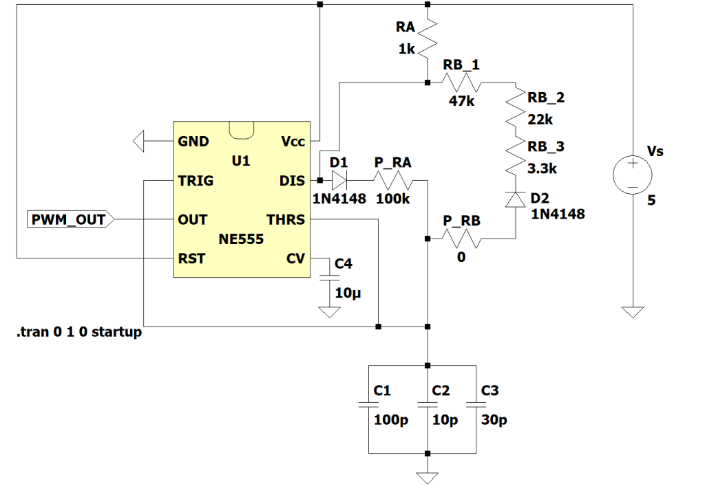
- Figure 13: Schematic for 555 Timer circuit with D = 0.583.
-
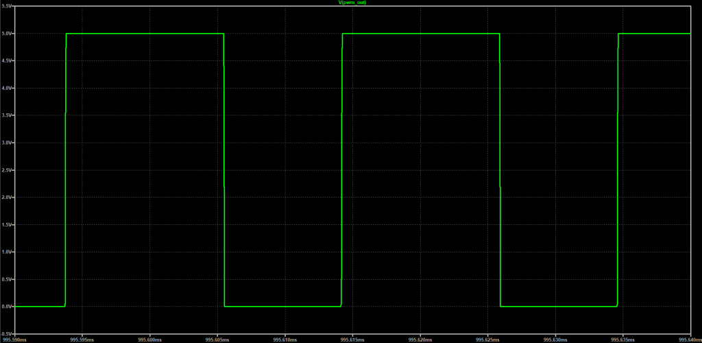
- Figure 14: Output waveform for 555 Timer circuit with D = 0.583.
-
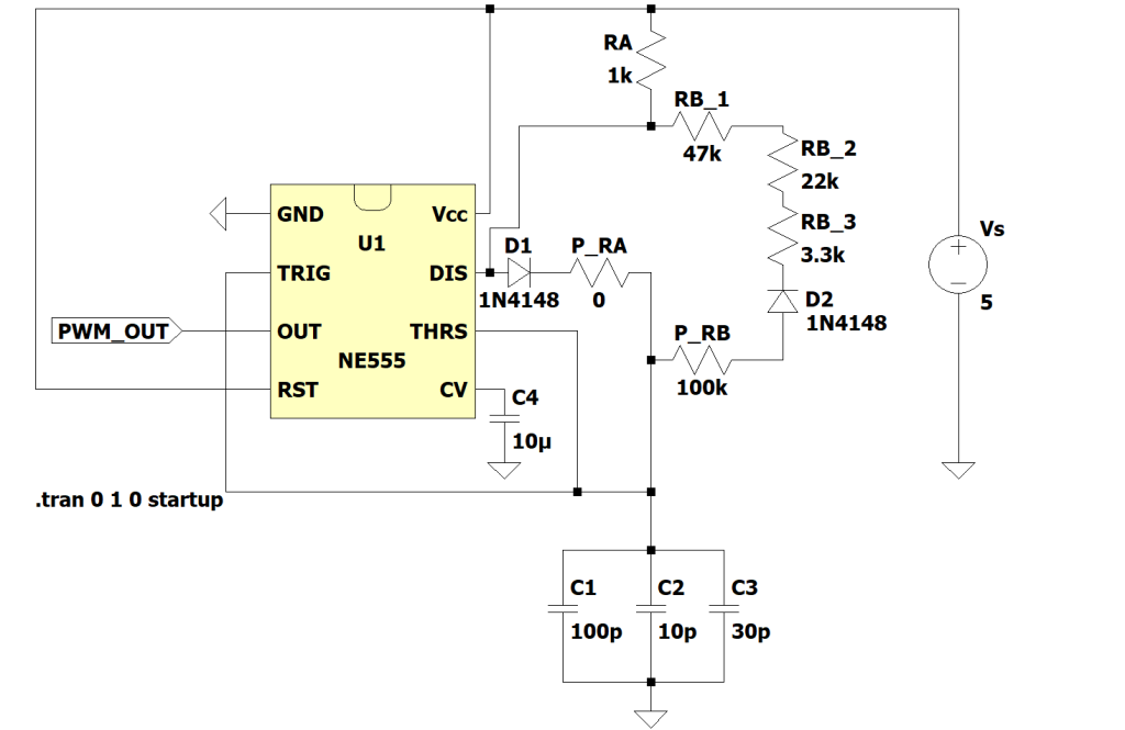
- Figure 15: Schematic for 555 Timer circuit with ~D = 0.
-
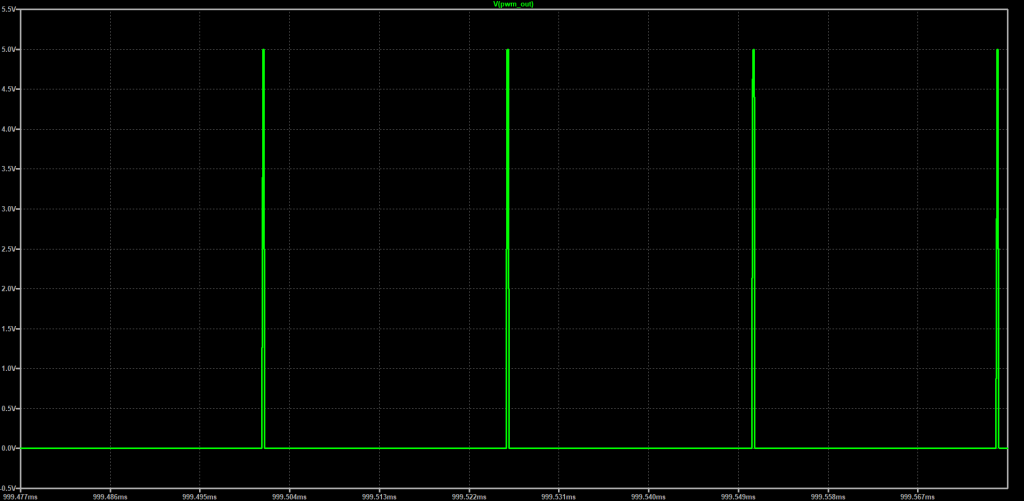
- Figure 16: Output waveform for 555 Timer circuit with ~D = 0.
Results:
To verify the performance of the circuit that I created, I captured the waveforms of the output voltage of the 555 timer segment of the circuit and the output voltage of the boost converter portion corresponding to the minimum and maximum duty cycles of the 555 timer. The input voltage for the circuit was 5V and at a duty cycle of ~1.5%, the measured output voltage was around 4.79V. This aligns with the expected behavior of a boost converter, as the lower the input duty cycle, the closer to the input voltage the output voltage becomes.
At a duty cycle of ~56.2%, the measured output voltage was around 10.1V. This differs by roughly 1.7V from the observed average voltage of the simulated LTSpice circuit, likely due to several non-ideal factors: losses from circuit components, the slower than expected switching frequency of the 555 timer output, and the lower maximum duty cycle observed from the output of the 555 timer. At the same duty cycle (~56.2%), the measured ripple current was around 54.7mV, which is almost triple the expected value. The increase in ripple voltage suggests that the observed slower switching frequency may have played a large impact in the discrepancy of the observed output voltage vs expected voltage. Additional discrepancies could be attributed to sources of loss, including losses in the physical resistance of the inductors / capacitors, as well as losses due to interconnecting wires for the breadboard. The following figures show the observed waveforms and measured values for the physical circuit (Figures 17-22):
-
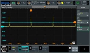
- Figure 17: Output waveform of converter at a duty cycle of 1.5% (blue) and the pulse output of 555 timer (yellow).
-
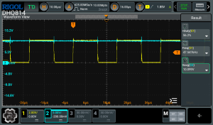
- Figure 18: Output waveform of converter at a duty cycle of 56.2% (blue) and the pulse output of 555 timer (yellow).
-
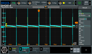
- Figure 19: Ripple behavior of the output voltage. at a duty cycle of 1.5% (blue).
-
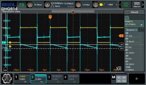
- Figure 20: Ripple behavior of the output voltage. at a duty cycle of 56.2% (blue).
-
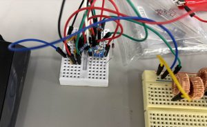
- Figure 21: Picture of physical 555 timer circuit on mini breadboard.
-
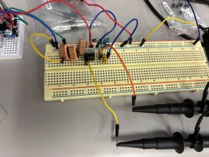
- Figure 22: Picture of physical boost converter circuit on breadboard..
Overall, the results demonstrated that this design of a boost converter will successfully boost an input voltage of 5V to an adjustable output in a range of ≈ 4.8V – 10.1V. In the event that a higher output voltage was desired, the potentiometer value can be increased to a larger range (i.e. 200kΩ pot instead of a 100kΩ).
References:
[1] A.S. Sedra and K. C. Smith, Microelectronic Circuits, 7th ed. New York, NY, USA: Oxford University Press, 2015.
[2] B. Yang, “Multivibrators” EE 331: Fundamentals of Electronics and Semiconductors. Western Carolina University, Fall 2024. (Lecture Notes).
[3] F. Dostal, “Selecting the Right Inductor Current Ripple,” Analog Devices, Mar. 6, 2023. [Online]. Available: https://www.analog.com/en/resources/technical-articles/selecting-the-right-inductor-current-ripple.html
[4] F. Stasi, “Working with Boost Converters,” Application Report SNVA731, Texas Instruments, June 2015. [Online]. Available: https://www.ti.com/lit/an/snva731/snva731.pdf
[5] N. Mohan, Power Electronics, A First Course: Simulations and Laboratory Implementations, 2nd ed. Hoboken, NJ, USA: John Wiley & Sons, 2023.
Recent Comments